![]()
 |
Application: | All high-density boards |
| Product Features: | Small surface mount, Solid state Faster time to trip than standard SMD devices Lower resistance than standard SMD devices | |
| Operation Current: | 140mA~1.6A | |
| Maximum Voltage: | 6V~60V | |
| Temperature Range: | -40°C to 85°C | |
| Agency Recognition: | UL (E211981), TÜV (R50004084) |
|
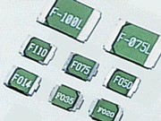
Part Number |
Hold Current |
Trip Current |
Rated Voltage |
Max Current |
Typical Power |
Max Time to Trip |
Resistance Tolerance | ||
|
Current |
Time |
RMIN |
R1MAX | ||||||
|
IH, A |
IT, A |
VMAX, Vdc |
IMAX, A |
Pd, W |
Amp |
Sec |
Ω |
Ω | |
|
FSMD014 |
0.14 |
0.30 |
60 |
10 |
0.8 |
8.0 |
〈0.02 |
1.50 |
6.50 |
|
FSMD020 |
0.20 |
0.40 |
30 |
10 |
0.8 |
8.0 |
0.02 |
0.80 |
5.00 |
|
FSMD035 |
0.35 |
0.70 |
16 |
40 |
0.8 |
8.0 |
0.10 |
0.32 |
1.50 |
|
FSMD050 |
0.50 |
1.00 |
16 |
40 |
0.8 |
|
0.15 |
0.15 |
1.00 |
|
FSMD075 |
0.75 |
1.50 |
16 |
40 |
0.8 |
8.0 |
0.02 |
0.11 |
0.45 |
|
FSMD110 |
1.10 |
2.20 |
6 |
40 |
0.8 |
8.0 |
0.30 |
0.04 |
0.21 |
|
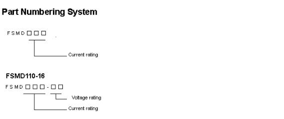
FSMD110-16 |
1.10 |
1.95 |
16 |
40 |
0.8 |
8.0 |
0.50 |
0.04 |
0.18 |
|
FSMD150 |
1.50 |
3.00 |
6 |
40 |
0.8 |
8.0 |
0.50 |
0.04 |
0.11 |
|
FSMD160 |
1.60 |
3.20 |
6 |
40 |
0.8 |
8.0 |
〈0.5 |
0.03 |
0.10 |
|
FSMD200 |
2.00 |
3.50 |
8 |
40 |
0.8 |
8.0 |
2 |
0.02 |
0.07 |
IH=Hold current-maximum current at which the device will not trip at 23℃still air.
IT=Trip current-minimum current at which the device will always trip at 23℃ still air.
V MAX=Maximum voltage device can withstand without damage at it rated current.(I max)
I MAX= Maximum fault current device can withstand without damage at rated voltage (V max).
Pd=Typical power dissipated-type amount of power dissipated by the device when in the tripped state in 23℃ still air environment.
RMIN=Minimum device resistance at 23℃ prior to tripping.
R1MAX=Maximum device resistance at 23℃ measured 1 hour post trip.
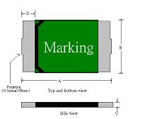
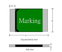
Termination pad characteristics
Termination pad materials: Tin-plated copper
 | |||||||||||||||||||||||||||||||||||||||||||||||||||||||||||||||||||||||||||||||||||||||||||||||||||||||||||
|
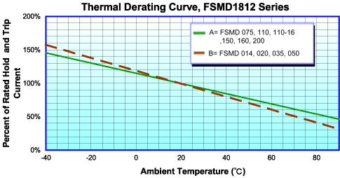
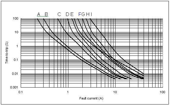
A =FSMD014 B =FSMD020 C =FSMD035 D =FSMD050 E =FSMD075 F =FSMD110-16 G = FSMD110 H =FSMD150 I =FSMD160 J=FSMD200 |
|
![]()
|
| Warning: |
|
|
|
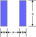
| Pad Layouts,
Solder Reflow and Rework Recommendations The dimension in the table below provide the recommended pad layout for each FSMD1812 device | |||||||||||||||||||||||||||||||||||||||||||||||||
 |
| ||||||||||||||||||||||||||||||||||||||||||||||||
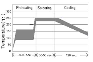 |
Solder reflow Due to “Lead Free” nature, up to 40 seconds Dwelling time for the soldering zone is strongly recommend . 1. Recommended reflow methods; IR, vapor phase oven, hot air oven. 2. The FSMD1812 Series are suitable for use with wave-solder application methods. 3. Recommended maximum paste thickness is 0.25mm. 4. Devices can be cleaned using standard industry methods and solvents. CAUTION: Rework: All the specifications are subject to change without previous notice. | ||||||||||||||||||||||||||||||||||||||||||||||||